ECE121 Experiment No. 2 - SCR Gate Characteristics
SCR GATE CHARACTERISTICS
Laboratory Exercise No. 2
Performance Objectives
A. Demonstrate the effect of negative gate current in an SCR.
B. Demonstrate the effect of excess capacitance in the gate circuit of an SCR.
C. Demonstrate the effect of inadequate energy in the trigger signal of an SCR.
Basic Concepts
1. Negative gate current can cause an SCR to turn off.
2. Too much capacitance in the gate circuit tends to hold the SCR on.
3. Inductance and capacitance in the gate circuit can cause an SCR to oscillate.
4. A trigger signal can be any shape but must have both the proper amplitude and width to trigger an SCR.
Equipment and Materials
ü Power Source 0-6 Vdc, 10mA
ü Power Source 6.3 Vac, 150mA
ü Milliammeter 0-10mAdc
ü Electronic VOM
ü Bread board
ü C1 50μf Electrolytic
ü DS1 Miniature Lamp
ü Q1 SCR, C106B1
ü R1, R3 1KΩ, 1W
ü R2 10KΩ, 1W
ü R5, R6 47KΩ, 1W
ü S1 SPST component module
ü S2 PBNO component module
ü S3 DPST component module
Objective A. Demonstrate the effect of negative gate current in an SCR.
1. a) Examine the circuit shown in Fig. 1. Switch S1 is used to apply anode-to-cathode voltage VAK. The milliammeter measures the combined anode and gate current. Switch S2 is used in conjunction with voltage divider R1-R2 to apply a gate trigger to Q2. R2 serves the additional purpose of bypassing gate leakage current around the gate-cathode PN junction. This decreases the gate triggering sensitivity but reduces the possibility of self-triggering or false triggering of the SCR due to leakage current. R3 is the load resistor. Switch S3 connects the negative power supply voltage to the gate. Connect the circuit shown. Be sure S1 and S3 are open.
Figure 1
b) Adjust the VAK power supply to 6Vdc. Be sure the negative power supply voltage applied to the gate is zero.
c) Close switch S1.
d) Momentarily depress S2. Record the milliammeter indication.
IA = 5 mAdc
e) Set the Electronic VOM to the 5Vdc range and connect it across the output of the negative power supply.
f) Close S3.
g) Very slowly increase the negative voltage applied to the gate until the milliammeter monitoring anode current drops to zero. Stop increasing the voltage at this point. This should occur at approximately -2.5Vdc. Do not exceed –Vdc as this is the SCR gate-cathode reserve breakdown voltage rating.
h) Yes, the SCR is turned off.
i) Describe what caused the SCR to turn off.
There is a negative current entering the gate.
j) Open S1 and S3 and reduce both power supplies to zero.
Objective B. Demonstrate the effect of excess capacitance in the circuit of an SCR.
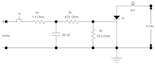
2. a) Examine the circuit shown in Fig. 2. Depressing S2 triggers the SCR. Without C1 in the circuit, the SCR turns on when triggered and remains on for the positive alternation of the 6.3Vac anode-to-cathode voltage. During this time DS1 lights. When S1 is released, the SCR is reverse biased on the negative alternation and turn off. Connect the circuit as shown but do not connect C1.
b) Adjust VAK to 6.3Vac. Adjust the dc power supply to 6Vdc.
c) Depress and hold S2. Is DS1 lit? Yes
d) Release S2. Does DS1 go out? Yes
e) Connect 50μF capacitory C1 as shown in Fig. 2.
f) Now depress and release S2. Does DS1 light remain on? Explain.
Yes, DS1 lamp remains on because of the capacitor.
g) Can you conclude that too much capacitance in the gate circuit produces improper operation?
h) Reduce all voltage sources to zero.
Conclusion
Labels: ece121 industrial electronics, silicon controlled rectifier


3 Comments:
i can see any pictures of the circuit..,hehe
December 7, 2012 at 3:08 PM
please please share diagram also please
October 4, 2017 at 4:39 AM
circuit diagram is missing
December 8, 2020 at 8:30 PM
Post a Comment
Subscribe to Post Comments [Atom]
<< Home